上海理工大学 光电信息与计算机工程学院,上海 200093
为了研究部分刻蚀光栅对波导光栅衍射光束的影响,提高集成光子学设计自由度,通过有限时域差分法仿真分析了分别在光栅边缘或中间进行波导部分刻蚀后的不同结构的性质,输入光波长为1 400~1 700 nm,覆盖1 550 nm通信波长,仿真结果表明:边缘刻蚀方法具有更高的辐射率、更低的反射率,并且可以控制辐射光场的强度分布;中间刻蚀方法波导中的反射能量更强且线宽更窄。2种刻蚀方法下,光栅尺寸越大则辐射率越高;当光栅尺寸固定,波导宽度越大则边缘刻蚀的辐射率越低。波导光栅的部分刻蚀方法可以用于集成光路的设计优化。
绝缘体上硅 光栅 波导 集成光学 silicon-on-insulators grating waveguide integrated optics 
Author Affiliations
Abstract
1 University of Shanghai for Science and Technology, Terahertz Technology Innovation Research Institute, Shanghai Key Laboratory of Modern Optical System, Shanghai, China
2 Shanghai Jiao Tong University, State Key Laboratory of Advanced Optical Communication Systems and Networks, Department of Electronic Engineering, Shanghai, China
We propose a terahertz (THz) vortex emitter that utilizes a high-resistance silicon resonator to generate vortex beams with various topological charges. Addressing the challenge of double circular polarization superposition resulting from the high refractive index contrast, we regulate the transverse spin state through a newly designed second-order grating partially etched on the waveguide’s top side. The reflected wave can be received directly by a linearly polarized antenna, simplifying the process. Benefiting from the tuning feature, a joint detection method involving positive and negative topological charges identifies and detects rotational Doppler effects amid robust micro-Doppler interference signals. This emitter can be used for the rotational velocity measurement of an on-axis spinning object, achieving an impressive maximum speed error rate of ∼2 % . This approach holds promise for the future development of THz vortex beam applications in radar target detection and countermeasure systems, given its low cost and potential for mass production.
vortex beam emitter terahertz rotational Doppler detection Advanced Photonics
2023, 5(6): 066002

Author Affiliations
Abstract
1 Terahertz Technology Innovation Research Institute, Terahertz Spectrum and Imaging Technology Cooperative Innovation Center, Shanghai Key Laboratory of Modern Optical System, University of Shanghai for Science and Technology, Shanghai 200093, China
2 Shanghai Institute of Intelligent Science and Technology, Tongji University, Shanghai 200092, China
Low-loss dielectric terahertz (THz) chips are efficient platforms for diverse THz applications. One of the key elements in the chip is the coupler. Most of the available THz couplers are in-plane and couple the THz wave from the metal waveguide to the dielectric waveguide. However, out-of-plane couplers are more suitable for wafer-scale testing and tolerant of alignment variation. In this work, we propose an out-of-plane THz coupler for coupling the antenna to the dielectric waveguide. The device is constructed using a grating and a compact spot-size converter. As the conventional optical spot-size converters that apply directly to THz chips are too large, we have designed a compact spot-size converter based on a tapered waveguide with a lens. The total device is 2.9 cm long and can couple a 7 mm diameter THz beam to a 500 µm wide waveguide. The device can scan the THz beam, radiate the input rectangular waveguide mode to free space, and drive the rotation angle of the fan beam through the scanning frequency. We fabricated the device using a single lithography step on a silicon wafer. The out-of-plane coupling efficiency was found to be ∼5 dB at 194 GHz. The fan-beam steering range was found to be around 40° in the frequency range of 170–220 GHz. The proposed out-of-plane coupling technique may provide an effective way for THz wafer-scale testing with a higher degree of freedom for on-chip integration. Also, the proposed technique being non-mechanical, beam steering using it, may therefore find applications in THz radar, communication, and sensing.
terahertz device grating coupler spot-size converter beam steering Chinese Optics Letters
2022, 20(2): 021301
上海理工大学 光电信息与计算机工程学院,上海 200093
集成太赫兹滤波器是实现集成太赫兹通信系统的基本器件之一,为了使太赫兹滤波器实现片上可调,提出了基于温控系统的太赫兹可调谐滤波器。相比于其他的太赫兹滤波器,提出的片上可调谐滤波器的调谐方法简单,尺寸小,可以很好地与其他太赫兹器件集成到晶片上。利用温控系统改变晶片的温度,再利用硅材料的热光效应改变折射率,使得微环耦合状态发生变化,从而让太赫兹滤波器的谐振峰发生漂移。在将加热片从30 ℃逐渐加温到90 ℃的过程中,太赫兹可调谐滤波器在180 GHz附近的谐振峰中心频率从180.453 GHz逐渐减小到180.224 GHz,变化范围为0.229 GHz,谐振深度从−68 dB逐渐变化为−44 dB,半高宽由原来的0.040 GHz逐渐变为0.246 GHz。
太赫兹波 滤波器 温控系统 集成太赫兹器件 terahertz filter temperature control system integrated terahertz devices
上海理工大学 光电信息与计算机工程学院,上海 200093
随着通信技术的飞速发展,传统微电子行业出现瓶颈,人们更多地寄希望于集成光路来实现新的突破。硅基光子学因其自身材料以及制造工艺等方面的优点而备受关注。其中,硅基耦合器作为重要的硅基无源器件,是实现光的片上合束和分束的关键。多模干涉(multimode interference, MMI)耦合器具有损耗低,工艺容差性大且带宽较大等优点,是一种常用的集成光学器件。从MMI耦合器的自映像成像原理出发,利用导模传输分析法(guide-mode propagation analysis, G-MPA)对MMI中的模场分布情况进行分析,成功设计出基于470 μm高阻硅晶圆的太赫兹波段的taper型多模干涉耦合器。通过时域有限差分法(finite difference time domain method, FDTD)仿真优化其参数,实现了93.8%的耦合效率。
太赫兹 taper 自映像 多模干涉(MMI)耦合器 terahertz taper self-image imaging multimode interference coupler 
Author Affiliations
Abstract
1 Terahertz Technology Innovation Research Institute, Terahertz Spectrum and Imaging Technology Cooperative Innovation Center, Shanghai Key Laboratory of Modern Optical System, University of Shanghai for Science and Technology, Shanghai 200093, China
2 Shanghai Institute of Intelligent Science and Technology, Tongji University, Shanghai 200092, China
3 Focused Photonics (Hangzhou) Inc, Hangzhou 310052, China
4 Suzhou H&L Instruments LLC, Suzhou 215123, China
5 e-mail: ymzhu@usst.edu.cn
The control of spin electromagnetic (EM) waves is of great significance in optical communications. Although geometric metasurfaces have shown unprecedented capability to manipulate the wavefronts of spin EM waves, it is still challenging to independently manipulate each spin state and intensity distribution, which inevitably degrades metasurface-based devices for further applications. Here we propose and experimentally demonstrate an approach to designing spin-decoupled metalenses based on pure geometric phase, i.e., geometric metasurfaces with predesigned phase modulation possessing functionalities of both convex lenses and concave lenses. Under the illumination of left-/right-handed circularly polarized (LCP or RCP) terahertz (THz) waves, these metalenses can generate transversely/longitudinally distributed RCP/LCP multiple focal points. Since the helicity-dependent multiple focal points are locked to the polarization state of incident THz waves, the relative intensity between two orthogonal components can be controlled with different weights of LCP and RCP THz waves, leading to the intensity-tunable functionality. This robust approach for simultaneously manipulating orthogonal spin states and energy distributions of spin EM waves will open a new avenue for designing multifunctional devices and integrated communication systems.
Photonics Research
2021, 9(6): 06001019
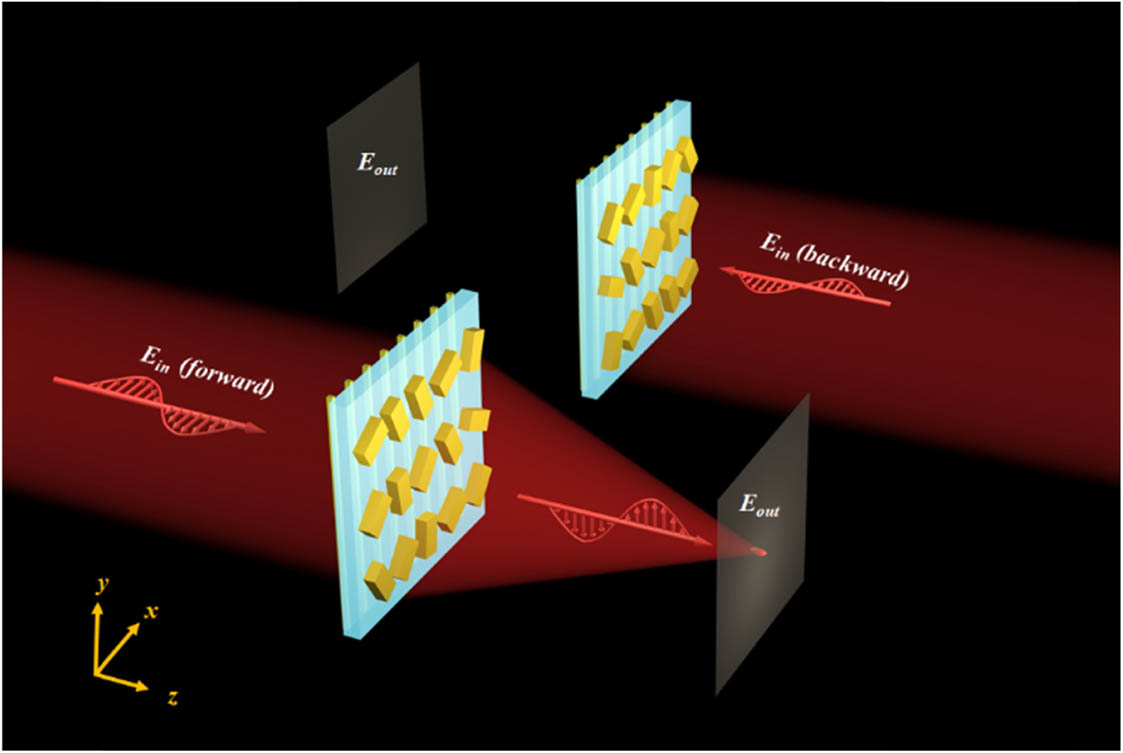
Author Affiliations
Abstract
1 Terahertz Technology Innovation Research Institute, Terahertz Spectrum and Imaging Technology Cooperative Innovation Center, Shanghai Key Laboratory of Modern Optical System, University of Shanghai for Science and Technology, Shanghai 200093, China
2 Shanghai Institute of Intelligent Science and Technology, Tongji University, Shanghai 200092, China
3 e-mail: ymzhu@usst.edu.cn
Asymmetric transmission, defined as the difference between the forward and backward transmission, enables a plethora of applications for on-chip integration and telecommunications. However, the traditional method for asymmetric transmission is to control the propagation direction of the waves, hindering further applications. Metasurfaces, a kind of two-dimensional metamaterials, have shown an unprecedented ability to manipulate the propagation direction, phase, and polarization of electromagnetic waves. Here we propose and experimentally demonstrate a metasurface-based directional device consisting of a geometric metasurface with spatially rotated microrods and metallic gratings, which can simultaneously control the phase, polarization, and propagation direction of waves, resulting in asymmetric focusing in the terahertz region. These dual-layered metasurfaces for asymmetric focusing can work in a wide bandwidth ranging from 0.6 to 1.1 THz. The flexible and robust approach for designing broadband asymmetric focusing may open a new avenue for compact devices with potential applications in encryption, information processing, and communication.
Photonics Research
2020, 8(6): 06000830


